Nano-image printing technology has exceeded the limit of microelectronics production accuracy (micron level), and has advanced electronics and printing to the microscopic nano-processing scale. Nowadays, in the field of map printing and production, the application of nanotechnology, the printing and production of micro-nano maps, has gradually matured. Now briefly introduce the classification and production technology of micro-nano maps.
1. Micro-nano map features and classification
Ordinary maps are graphs or images that selectively represent several phenomena on a flat or spherical surface in two-dimensional or multi-dimensional forms and means, and scientifically reflect the distribution characteristics of natural and social economic phenomena. The micro-nano map is completely different from the map, its size is tiny, only a few hundred nanometers to a few microns. High-power optical microscopy equipment is needed to see the outline of the map clearly. It does not contain information on natural and socio-economic phenomena.
Micro-nano maps are new things that have emerged in recent years. Micro-nano maps can be divided into plan view (Figure 1) and perspective view (Figure 2). Figure 1 is a planar nanoscale map of China etched by scientists using the scanning tunneling microscope (STM) probe tip of the Institute of Chemistry, Chinese Academy of Sciences. The line thickness of the map is about 10 μm, and the overall size is hundreds of nanometers. Figure 2 is a 3D nano world map recently developed by scientists from IBM in the United States. The figure is based on the surface of a high-molecular polymer, about 22μm × 11μm, contains a total of 500,000 pixels, and the area of ​​each pixel is 20μm2. The mountain range with an altitude of 1000m is only 8μm in the figure, which means that Mount Everest is only 64μm high in the figure.
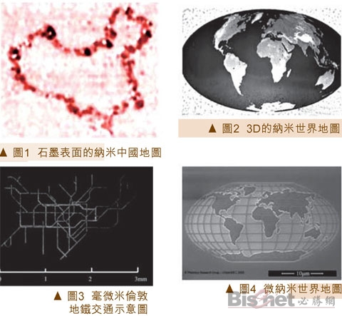
Micro-nano maps can be divided into three categories: nanometer level, micro-nano level, and nano-level. Figure 3 is the masterpiece of the British Nanobiology Consulting Center (BNC) scientist-the world's smallest nanometer-level London subway traffic map. The material used is 3mm × 2mm single crystal silicon, and the subway line is about tens of microns wide; it is processed by Oxford laser engraving system. Figure 4 is a 1: 1000 billion micro-nano-scale world map made by scientists at the Optical Center of Ghent University in Belgium. It is imaged using an electron microscope and produced by traditional optical lithography in microelectronics. The equator is about 40 μm long. Figure 5 is a nanoscale world map made by American scientists using tungsten deposited on a silicon nitride film by an electron beam. The equator is only 230 μm long. Figure 6 is the nanomap of Taiwan region that won the 2006 Taiwan Micro Image Contest, and Figure 7 is the nanomap of the African continent that won the first international nanoart exhibition. They are all imaged using a scanning tunneling microscope, which is drawn on the surface of titanium and silicon by applying current through the probe, and the map size is only a few hundred nanometers. Among them, Figure 7 is a nano-Africa map made by two well-known pioneers of nano-arts-Italy's A lessandro o Scali and South Africa's Robin Goode. Materials for making micro-nano maps include semiconductors, biology, polymers, metals, and carbon. Nanomaps made of semiconductor materials are the most common. Figure 8 is a nano-China map of biological materials (biological DNA chain)-DNA China map. The technology used is advanced DNA origami, and the overall size of the map is about a few hundred nanometers.
The creation mechanism of micro-nano maps can be divided into works based on physical methods and based on chemical methods. The maps in Figures 1-8 belong to micro-nano maps made based on chemical methods, because in their manufacturing methods, they involve the oxidation of materials, the decomposition of polymers, corrosion washing, chemical vapor deposition, or the polymerization of DNA. Figure 9 is a nano-map of Taiwan made entirely based on the physical method, using the tip of an atomic force microscope (AFM) probe to depict the copper crystal surface and imaged with AFM. This picture is the award-winning work of the 2006 Taiwan Micro Image Contest.
[PROFESSIONAL & LARGE CAPACITY] As the continuation of TARION PB camera bag series, this large camera backpack features professional with a large capacity of 1 camera + 5 lens easily. All the inner padded dividers can be reorganized, even the top and bottom compartments can be changed into one to hold anything about the size of a handheld stabilizer etc.. Side pocket can carry tripod and assisted by side straps. Plenty of accessory pockets for SD cards, cables, batteries and others.
[QUICK SIDE ACCESS & DEDICATED LAPTOP COMPARTMENT] The large camera bag with side access compartment allows for reaching the gear in a short time without taking off the big camera backpack, never miss the fleeting moment. Dedicated back computer sleeve fits up to 15.6 inch thin laptops.
[SHOCK-PROOF & ABRASION- AND WEATHER-RESISTANT] Thickened protective pad inside, shockproof and no deformed help protect your camera & lens safety and security. High density nylon which boasts anti-tear and water resistant properties, all weather protection with waterproof raincover.
[ERGONOMIC BACK-SUPPORT] Rear padded air mesh panel and ergonomic design increase airflow while hiking or traveling and distribute the weight evenly to add comfort and save energy especially use this hiking camera backpack fully loaded on the go.
[OUTDOOR PHOTOGRAPHY FRIENDLY] Made of water repellency and high strength tear-resistance nylon, this large camera bag is sturdy and durable, attached an extra rain cover for this outdoor photography backpack keeps rain and dust out, makes it one of a kind storm-proof backpack that can take whatever weather throws at it.
Carry on backpack,foldable backpack, luggage backpack, suitcase backpack, laptop travel bag, cute travel backpacks, travel backpack, camera backpack, large camera bag, picnic backpack, mommy backpack
Zhejiang Yinglin Luggage Co. Ltd , https://www.yllcluggages.com